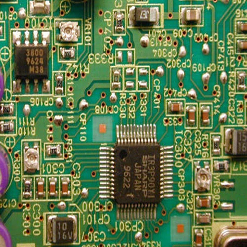
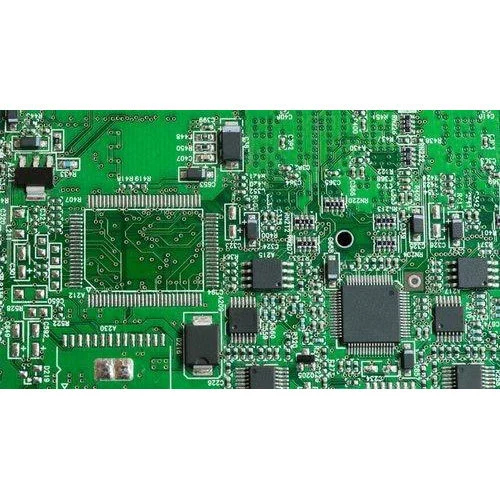
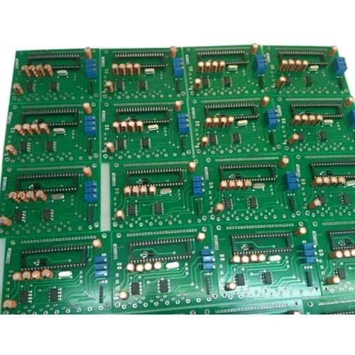
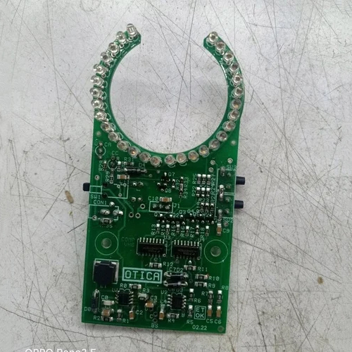
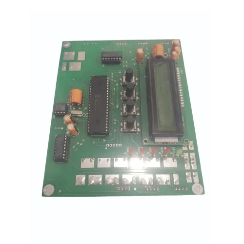
About 10 X 20cm PCB Design Service
Industries Served:
- Consumer Electronics
- Industrial Equipment
- Medical Devices
- Automotive
- Telecommunications
- IoT (Internet of Things)
Benefits:
- Optimized for Size and Performance: We deliver a compact 10 x 20 cm design that maximizes space without sacrificing performance, ensuring your PCB fits perfectly within the intended device.
- Cost-Effective Design: Our design approach prioritizes both performance and cost-efficiency, ensuring that you get the best value for your project.
- Expert Engineering: Our experienced design team ensures that your PCB is crafted with the highest attention to detail, providing reliable performance and ease of manufacture.
- Fast Turnaround: We understand the importance of meeting deadlines and provide quick turnaround times without compromising quality.
Optimized Design for Versatile ApplicationsWhether for industrial automation, prototyping, or consumer devices, the 10 x 20cm PCB Design Service offers flexible solutions. Choose single or double layered boards, specify custom shapes, and leverage impedance-controlled layouts to match your applications requirements. Each PCB strictly adheres to IPC Class 2 standards and is RoHS compliant, ensuring both quality and environmental safety.
Comprehensive Software and Format SupportOur service works seamlessly with leading PCB design toolsAltium, Eagle, KiCAD, OrCADand delivers precise Gerber files for manufacturing. This compatibility offers engineers the freedom to use their preferred software environment without sacrificing consistency or quality in the final product.
Turnkey Project Management and Technical SupportFrom initial design to final testing, our experienced engineers guide every step of the process. Optional board testing and full technical support ensure any issues are addressed promptly, allowing for a hassle-free, reliable experience for both new and established clients.
FAQs of 10 X 20cm PCB Design Service:
Q: How does the 10 x 20cm PCB Design Service accommodate different design softwares?
A: Our service is compatible with Altium, Eagle, KiCAD, and OrCAD. You can submit your design files in these formats, and we ensure that Gerber files are generated to meet manufacturing standards without loss of fidelity.
Q: What is the typical turnaround time for PCB design and delivery?
A: Production and design are completed within 7 to 10 days, enabling quick development cycles for both prototypes and batch manufacturing.
Q: When is testing service available for ordered PCBs?
A: Testing services can be requested at the time of order. Our engineers conduct thorough checks to verify board functionality and compliance before delivery.
Q: Where is the 10 x 20cm PCB Design Service available?
A: We provide our PCB design and manufacturing services across India, catering to manufacturers, service providers, suppliers, and traders.
Q: What process is followed from design submission to final delivery?
A: Once you submit your design files, our team reviews and optimizes the layout for manufacturability. We generate Gerber files, commence fabrication using your specifications, and, if requested, conduct board testing before final delivery.
Q: How does this service benefit product developers and manufacturers?
A: Developers benefit from experienced technical support, fast lead times, robust quality controls (IPC Class 2, RoHS), and customization options such as impedance control, plated through-hole vias, and tailored shapes for their specific projects.
Q: Can custom PCB shapes and impedance control be requested in this service?
A: Yes, we accommodate custom board shapes and specific impedance requirements. Simply provide your details during the design phase for implementation.